Symbol Names: NMOS, NMOS3, PMOS, PMOS3There are two fundamentally different types of MOSFETS in LTspice, monolithic MOSFETs and a new vertical double diffused power MOSFET model.
Monolithic MOSFET:
Syntax: Mxxx Nd Ng Ns Nb <model> [m=<value>] [L=<len>]
+ [W=<width>] [AD=<area>] [AS=<area>]
+ [PD=<perim>] [PS=<perim>] [NRD=<value>]
+ [NRS=<value>] [off] [IC=<Vds, Vgs, Vbs>]
+ [temp=<T>]
M1 Nd Ng Ns 0 MyMOSFET
.model MyMOSFET NMOS(KP=.001)
M1 Nd Ng Ns Nb MypMOSFET
.model MypMOSFET PMOS(KP=.001)
Vertical double diffused power MOSFET:
Syntax: Mxxx Nd Ng Ns <model> [L=<len>] [W=<width>]
+ [M=<area>] [m=<value>] [off]
+ [IC=<Vds, Vgs, Vbs>] [temp=<T>]
Example:
M1 Nd Ng Ns Si4410DY
.model Si4410DY VDMOS(Rd=3m Rs=3m Vto=2.6 Kp=60
+ Cgdmax=1.9n Cgdmin=50p Cgs=3.1n Cjo=1n
+ Is=5.5p Rb=5.7m)
The MOSFET's model card specifies which type is intended. The model card keywords NMOS and PMOS specify a monolithic N- or P- channel MOSFET transistor. The model card keyword VDMOS specifies a vertical double diffused power MOSFET.
Monolithic MOSFETS are four terminal devices. Nd, Ng, NS, and Nb are the drain, gate, source, and bulk; i.e., substrate; nodes. L and W are the channel length and width, in meters. AD and AS are the areas of the drain and source diffusions, in square meters. Note that the suffix u specifies µm and p square µm. If any of L, W, AD, or AS are not specified, default values are used. PD and PS are the perimeters of the drain and source junctions, in meters. NRD and NRS designate the equivalent number of squares of the drain and source diffusions; these values multiply the sheet resistance RSH specified on the .MODEL control line. PD and PS default to zero while NRD and NRS to one. OFF indicates an initial condition on the device for DC analysis. The initial condition specification using IC=VDS, VGS, VBS is for use with the UIC option on the .TRAN control line, when a transient analysis is desired starting from other than the quiescent operating point. The optional TEMP value is the temperature at which this device is to operate, and overrides the temperature specification on the .OPTION control line. The temperature specification is ONLY valid for level 1, 2, 3, and 6 MOSFETs, not for level 4, 5 or 8 BSIM devices.
LTspice contains seven different types of monolithic MOSFET's and one type of vertical double diffused Power MOSFET.
There are seven monolithic MOSFET device models. The model parameter LEVEL specifies the model to be used. The default level is one.
level model
------------------------------------------------------
1 Shichman-Hodges
2 MOS2(see A. Vladimirescu and S. Liu, The Simulation of MOS Integrated Circuits Using SPICE2, ERL Memo No. M80/7, Electronics Research Laboratory University of California, Berkeley, October 1980)
3 MOS3, a semi-empirical model(see reference for level 2)
4 BSIM (see B. J. Sheu, D. L. Scharfetter, and P. K. Ko, SPICE2 Implementation of BSIM. ERL Memo No. ERL M85/42, Electronics Research Laboratory University of California, Berkeley, May 1985)
5 BSIM2 (see Min-Chie Jeng, Design and Modeling of Deep-Submicrometer MOSFETs ERL Memo Nos. ERL M90/90, Electronics Research Laboratory University of California, Berkeley, October 1990)
6 MOS6 (see T. Sakurai and A. R. Newton, A Simple MOSFET Model for Circuit Analysis and its application to CMOS gate delay analysis and series-connected MOSFET Structure, ERL Memo No. ERL M90/19, Electronics Research Laboratory, University of California, Berkeley, March 1990)
8 BSIM3v3.3.0 from University of California, Berkeley as of July 29, 2005
9 BSIMSOI3.2 (Silicon on insulator) from the BSIM Research Group of the University of California, Berkeley, February 2004.
12 EKV 2.6 based on code from Ecole Polytechnique Federale de Lausanne. See http://legwww.epfl.ch/ekv and "The EPFL-EKV MOSFET Model Equations for Simulation, Version 2.6", M. Bucher, C. Lallement, F. Theodoloz, C. Enz, F. Krummenacher, EPFL-DE-LEG, June 1997.
14 BSIM4.6.1 from the University of California, Berkeley BSIM Research Group, May 18, 2007.
The DC characteristics of the level 1 through level 3 MOSFETs are defined by the device parameters VTO, KP, LAMBDA, PHI and GAMMA. These parameters are computed if the process parameters(NSUB, TOX,...) are given, but user-specified values always override. VTO is positive (negative) for enhancement mode and negative (positive) for depletion mode N-channel (P-channel) devices. Charge storage is modeled by three constant capacitors, CGSO, CGDO, and CGBO which represent overlap capacitances, by the non-linear thin-oxide capacitance which is distributed among the gate, source, drain, and bulk regions, and by the nonlinear depletion-layer capacitances for both substrate junctions divided into bottom and periphery, which vary as the MJ and MJSW power of junction voltage respectively, and are determined by the parameters CBD, CBS, CJ, CJSW, MJ, MJSW and PB. Charge storage effects are modeled by the piecewise linear voltages-dependent capacitance model proposed by Meyer. The thin-oxide charge-storage effects are treated slightly different for the Level=1 model. These voltage dependent capacitances are included only if Tox is specified.
There is some overlap among the parameters describing the junctions, e.g., the reverse current can be specified either through Is[Amp] or through Js[Amp/m/m]. Whereas the first is an absolute value the second is multiplied by Ad and As to give the reverse current of the drain and source junctions respectively. The same idea applies also to the zero-bias junction capacitances CBD and CBS[Farad] on one hand, and CJ[Farad/m/m] on the other. The parasitic drain and source series resistance can be expressed as either RD and RS[Ohms] or RSH[Ohms/square], the latter being multiplied by the number of squares NRD and NRS input on the device line.
MOSFET level 1, 2, and 3 parameters:
|
Name |
Description |
Units |
Default |
Example |
|
Vto |
Zero-bias threshold voltage |
V |
0 |
1.0 |
|
Kp |
Transconductance parameter |
A/V² |
2e-5 |
3e-5 |
|
Gamma |
Bulk threshold parameter |
V^½ |
0. |
0.37 |
|
Phi |
Surface inversion potential |
V |
0.6 |
0.65 |
|
Lambda |
Channel-length modulation (level 1 and 2 only) |
1/V |
0. |
0.02 |
|
Rd |
Drain ohmic resistance |
W |
0. |
1. |
|
Rs |
Source ohmic resistance |
W |
0. |
1. |
|
Cbd |
Zero-bias B-D junction capacitance |
F |
0. |
20f |
|
Cbs |
Zero-bias B-S junction capacitance |
F |
0. |
20f |
|
Is |
Bulk junction saturation current |
A |
1e-14 |
1e-15 |
|
N |
Bulk diode emission coefficient |
- |
1. |
|
|
Pb |
Bulk junction potential |
V |
0.8 |
0.87 |
|
Cgso |
Gate-source overlap capacitance per meter channel width |
F/m |
0. |
4e-11 |
|
Cgdo |
Gate-drain overlap capacitance per meter channel width |
F/m |
0. |
4e-11 |
|
Cgbo |
Gate-bulk overlap capacitance per meter channel width |
F/m |
0. |
2e-10 |
|
Rsh |
Drain and source diffusion sheet resistance |
W |
0. |
10. |
|
Cj |
Zero-bias bulk junction bottom capacitance per square meter of junction area |
F/m² |
0. |
2e-4 |
|
Mj |
Bulk junction bottom grading coefficient |
- |
0.5 |
0.5 |
|
Cjsw |
Zero-bias bulk junction sidewall capacitance per meter of junction perimeter |
F/m |
0. |
1p |
|
Mjsw |
Bulk junction sidewall grading coefficient |
- |
.50 level 1 .33 level 2,3 | |
|
Js |
Bulk junction saturation current per square-meter of junction area |
A/m |
0. |
1e-8 |
|
Tox |
Oxide thickness |
m |
1e-7 |
1e-7 |
|
Nsub |
Substrate doping |
1/cm³ |
0. |
4e15 |
|
Nss |
Surface state density |
1/cm² |
0. |
1e+10 |
|
Nfs |
Fast surface state |
1/cm² |
0. |
1e+10 |
|
TPG |
Type of gate material: +1 opp. to substrate -1 same as substrate 0 Al gate |
- |
1 |
|
|
Xj |
Metallurgical junction depth |
m |
0. |
1µ |
|
Ld |
Lateral diffusion |
m |
0. |
0.8µ |
|
Uo |
Surface mobility |
cm²/V/s |
600 |
700 |
|
Ucrit |
Critical field for mobility degradation (level 2 only) |
V/cm |
1e4 |
1e4 |
|
Uexp |
Critical field exponent in mobility degradation (level 2 only) |
- |
0. |
0.1 |
|
Utra |
Transverse field coefficient (level 2 only) |
- |
0. |
0.3 |
|
Vmax |
Maximum carrier drift velocity (levels 2 & 3 only) |
m/s |
0. |
5e4 |
|
Neff |
Total channel-charge exponent (level 2 only) |
- |
1. |
5. |
|
Kf |
Flicker noise coefficient |
- |
0. |
1e-26 |
|
Af |
Flicker noise exponent |
- |
1. |
1.2 |
|
Fc |
Coefficient for forward-bias depletion capacitance formula |
- |
0.5 |
|
|
Delta |
Width effect on threshold voltage(levels 2 and 3) |
- |
0. |
1. |
|
Theta |
Mobility modulation (level 3 only) |
- |
0. |
0.1 |
|
Eta |
Static feedback (level 3 only) |
- |
0. |
1. |
|
Kappa |
Saturation field (level 3 only) |
|
0.2 |
0.5 |
|
Tnom |
Parameter measurement temperature |
ºC |
27 |
50 |
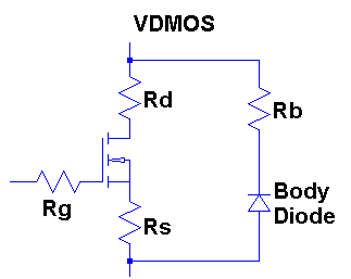
The discrete vertical double diffused MOSFET transistor(VDMOS) popularly used in board level switch mode power supplies has behavior that is qualitatively different than the above monolithic MOSFET models. In particular, (i) the body diode of a VDMOS transistor is connected differently to the external terminals than the substrate diode of a monolithic MOSFET and (ii) the gate-drain capacitance(Cgd) non-linearity cannot be modeled with the simple graded capacitances of monolithic MOSFET models. In a VDMOS transistor, Cgd abruptly changes about zero gate-drain voltage(Vgd). When Vgd is negative, Cgd is physically based a capacitor with the gate as one electrode and the drain on the back of the die as the other electrode. This capacitance is fairly low due to the thickness of the non-conducting die. But when Vgd is positive, the die is conducting and Cgd is physically based on a capacitor with the thickness of the gate oxide.
Traditionally, elaborate subcircuits have been used to duplicate the behavior of a power MOSFET. A new intrinsic spice device was written that encapsulates this behavior in the interest of compute speed, reliability of convergence, and simplicity of writing models. The DC model is the same as a level 1 monolithic MOSFET except that the length and width default to one so that transconductance can be directly specified without scaling. The AC model is as follows. The gate-source capacitance is taken as constant. This was empirically found to be a good approximation for power MOSFETS if the gate-source voltage is not driven negative. The gate-drain capacitance follows the following empirically found form:
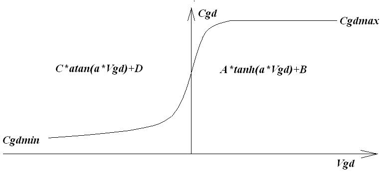
For positive Vgd, Cgd varies as the hyperbolic tangent of Vgd. For negative Vdg, Cgd varies as the arc tangent of Vgd. The model parameters a, Cgdmax, and Cgdmax parameterize the gate drain capacitance. The source-drain capacitance is supplied by the graded capacitance of a body diode connected across the source drain electrodes, outside of the source and drain resistances.
|
Name |
Description |
Units |
Default |
Example |
|
Vto |
Threshold voltage |
V |
0 |
1.0 |
|
Kp |
Transconductance parameter |
A/V² |
1. |
.5 |
|
Phi |
Surface inversion potential |
V |
0.6 |
0.65 |
|
Lambda |
Channel-length modulation |
1/V |
0. |
0.02 |
|
mtriode |
Conductance multiplier in triode region(allows independent fit of triode and saturation regions |
- |
1. |
2. |
|
subtreas |
Current(per volt Vds) to switch from square law to exponential subthreshold conduction |
A/V |
0. |
1n |
|
BV |
Vds breakdown voltage |
V |
Infin. |
40 |
|
IBV |
Current at Vds=BV |
A |
100pA |
1u |
|
NBV |
Vds breakdown emission coefficient |
- |
1. |
10 |
|
Rd |
Drain ohmic resistance |
W |
0. |
1. |
|
Rs |
Source ohmic resistance |
W |
0. |
1. |
|
Rg |
Gate ohmic resistance |
W |
0. |
2. |
|
Rds |
Drain-source shunt resistance |
W |
Infin. |
10Meg |
|
Rb |
Body diode ohmic resistance |
W |
0. |
.5 |
|
Cjo |
Zero-bias body diode junction capacitance |
F |
0. |
1n |
|
Cgs |
Gate-source capacitance |
F |
0. |
500p |
|
Cgdmin |
Minimum non-linear G-D capacitance |
F |
0. |
300p |
|
Cgdmax |
Maximum non-linear G-D capacitance |
F |
0. |
1000p |
|
A |
Non-linear Cgd capacitance parameter |
- |
1. |
.5 |
|
Is |
Body diode saturation current |
A |
1e-14 |
1e-15 |
|
N |
Bulk diode emission coefficient |
- |
1. |
|
|
Vj |
Body diode junction potential |
V |
1. |
0.87 |
|
M |
Body diode grading coefficient |
- |
0.5 |
0.5 |
|
Fc |
Body diode coefficient for forward-bias depletion capacitance formula |
- |
0.5 |
|
|
tt |
Body diode transit time |
sec |
0. |
10n |
|
Eg |
Body diode activation energy for temperature effect on Is |
eV |
1.11 |
|
|
Xti |
Body diode saturation current temperature exponent |
- |
3. |
|
|
L |
Length scaling |
- |
1. |
|
|
W |
Width scaling |
- |
1. |
|
|
Kf |
Flicker noise coefficient |
- |
0. |
|
|
Af |
Flicker noise exponent |
- |
1. |
|
|
nchan[*] |
N-channel VDMOS |
- |
(true) |
- |
|
pchan[*] |
P-channel VDMOS |
- |
(false) |
- |
|
Tnom |
Parameter measurement temperature |
ºC |
27 |
50 |
*]The model name VDMOS is used both for a N-channel and P-channel device. The polarity defaults to N-channel. To specify P-channel, flag the model with the keyword "pchan", e.g., ".model xyz VDMOS(Kp = 3 pchan)" defines a P-channel transistor.