Q. Bipolar Transistor
Symbol Names: NPN, PNP, NPN2, PNP2
Syntax: Qxxx Collector Base Emitter [Substrate Node] model [area] [off] [IC=<Vbe, Vce>] [temp=<T>]
Example:
Q1 C B E MyNPNmodel.model MyNPNmodel NPN(Bf=75)
Bipolar transistors require a model card to specify its characteristics. The model card keywords NPN and PNP indicate the polarity of the transistor.
The bipolar junction transistor model is an adaptation of the integral charge control model of Gummel and Poon. This modified Gummel-Poon model extends the original model to include several effects at high bias levels, quasi-saturation, and substrate conductivity. The model automatically simplifies to the Ebers-Moll model when certain parameters are not specified. The DC model is defined by the parameters Is, Bf, Nf, Ise, Ikf, and Ne which determine the forward current gain characteristics, Is, Br, Nr, Isc, Ikr, and Nc which determine the reverse current gain characteristics, and Vaf and Var which determine the output conductance for forward and reverse regions. Three ohmic resistances Rb, Rc and Re, are included, where Rb can be high current dependent. Base charge storage is modeled by forward and reverse transit times, Tf and Tr, the forward transit time Tf being bias dependent if desired; and nonlinear depletion layer capacitances, which are determined by Cje, Vje and Mje, for the B-E junction, Cjc, Vjc, and MJC for the B-C junction and Cjs, Vjs, and Mjs for the Collector- Substrate junction. The temperature dependence of the saturation current, Is, is determined by the energy gap, Eg, and the saturation-current temperature exponent, XTI. Additionally base current temperature dependence is modeled by the beta temperature exponent XTB in the new model. The values specified are assumed to have been measured at the temperature TNOM, which can be specified on the .OPTIONS control line or overridden by a specification on the .model line.
The BJT parameters used in the modified Gummel-Poon model are listed below.
Modified Gummel-Poon BJT Parameters
| Name | Description | Units | Default |
| Is | Transport saturation current | A | 1e-16 |
| Ibc | Base-collector saturation current | A | Is |
| Ibe | Base-emitter saturation current | A | Is |
| Bf | Ideal maximum forward beta | - | 100 |
| Nf | Forward current emission coefficient | - | 1. |
| Vaf | Forward Early voltage | V | Infin. |
| Ikf | Corner for forward beta high current roll-off | A | Infin. |
| nk | High current roll-off coefficient | - | .5 |
| Ise | B-E leakage saturation current | A | 0. |
| Ne | B-E leakage emission coefficient | - | 1.5 |
| Br | Ideal maximum reverse beta | - | 1. |
| Nr | Reverse current emission coefficient | - | 1. |
| Var | Reverse Early voltage | V | Infin. |
| Ikr | Corner for reverse beta high current roll-off | A | Infin. |
| Isc | B-C leakage saturation current | A | 0 |
| Nc | B-C leakage emission coefficient | - | 2 |
| Rb | Zero-bias base resistance | Ω | 0 |
| Irb | Current where base resistance falls halfway to its min value | A | Infin. |
| Rbm | Minimum base resistance at high currents | Ω | Rb |
| Re | Emitter resistance | Ω | 0. |
| Rc | Collector resistance | Ω | 0. |
| Cje | B-E zero-bias depletion capacitance | F | 0. |
| Vje | B-E built-in potential | V | 0.75 |
| Mje | B-E junction exponential factor | - | 0.33 |
| Tf | Ideal forward transit time | sec | 0. |
| Xtf | Coefficient for bias dependence of Tf | - | 0. |
| Vtf | Voltage describing Vbc dependence of Tf | V | Infin. |
| Itf | High-current parameter for effect on Tf | A | 0. |
| Ptf | Excess phase at freq=1/(Tf*2*Ω)Hz | ° | 0. |
| Cjc | B-C zero-bias depletion capacitance | F | 0. |
| Vjc | B-C built-in potential | V | 0.75 |
| Mjc | B-C junction exponential factor | - | 0.33 |
| Xcjc | Fraction of B-C depletion capacitance connected to internal base node | - | 1. |
| Xcjc2 | Fraction of B-C depletion capacitance connected between internal base node and extrinsic collector | - | 0 |
| extsub | Extrinsicness of more intrinsic collector node used for substrate capacitance charge division | - | 0 |
| Tr | Ideal reverse transit time | sec | 0. |
| Cjs | Zero-bias collector-substrate capacitance | F | 0. |
| Xcjs | Fraction of Cjs connected internally to Rc | F | 0. |
| Vjs | Substrate junction built-in potential | V | 0.75 |
| Mjs | Substrate junction exponential factor | - | 0. |
| Xtb | Forward and reverse beta temperature exponent | - | 0. |
| Eg | Energy gap for temperature effect on Is | eV | 1.11 |
| Xti | Temperature exponent for effect on Is | - | 3. |
| Kf | Flicker-noise coefficient | - | 0. |
| Af | Flicker-noise exponent | - | 1. |
| Fc | Coefficient for forward-bias depletion capacitance formula | - | 0.5 |
| subs | Geometry selector if LPNP is not used: 1 means vertical 2 means lateral | - | NPN: 1 PNP: 2 |
| BVcbo | Collector-base breakdown voltage | - | Infin. |
| nBVcbo | Collector-base breakdown voltage coefficient | - | 5 |
| BVbe | Base-emitter breakdown voltage | V | Infin. |
| Ibvbe | Current at base-emitter breakdown voltage | A | 1e-10 |
| nbvbe | Base-emitter breakdown coefficient | - | 1. |
| Tnom | Parameter measurement temperature | °C | 27 |
| Cn | Quasi-saturation temperature coefficient for hole mobility | 2.42 NPN 2.2 PNP | |
| D | Quasi-saturation temperature coefficient for scattering-limited hole carrier velocity | .87 NPN .52 PNP | |
| Gamma | Epitaxial region doping factor | 1e-11 | |
| Qco | Epitaxial region charge factor | Coul | 0. |
| Quasimod | Quasi-saturation flag for temperature dependence | - | (not set) |
| Rco | Epitaxial region resistance | Ω | 0. |
| Vg | Quasi-saturation extrapolated bandgap voltage at 0°K | V | 1.206 |
| Vo | Carrier mobility knee voltage | V | 10. |
| Tre1 | Re linear temperature coefficient | 1/°C | 0. |
| Tre2 | Re quadratic temperature coefficient | 1/°C2 | 0. |
| Trb1 | Rb linear temperature coefficient | 1/°C | 0. |
| Trb2 | Rb quadratic temperature coefficient | 1/°C2 | 0. |
| Trc1 | Rc linear temperature coefficient | 1/°C | 0. |
| Trc2 | Rc quadratic temperature coefficient | 1/°C2 | 0. |
| Trm1 | Rmb linear temperature coefficient | 1/°C | 0. |
| Trm2 | Rmb quadratic temperature coefficient | 1/°C2 | 0. |
| Iss | Substrate junction saturation current | A | 0. |
| Ns | Substrate junction emission Coefficient | - | 1. |
| Tvaf1 | Vaf linear temperature coefficient | 1/°C | 0. |
| Tvaf2 | Vaf quadratic temperature coefficient | 1/°C2 | 0. |
| Tvar1 | Var linear temperature coefficient | 1/°C | 0. |
| Tvar2 | Var quadratic temperature coefficient | 1/°C2 | 0. |
| Tikf1 | Ikf linear temperature coefficient | 1/°C | 0. |
| Tikf2 | Ikf quadratic temperature coefficient | 1/°C2 | 0. |
| Trbm1 | Rbm linear temperature coefficient | 1/°C | 0. |
| Trbm2 | Rbm quadratic temperature coefficient | 1/°C2 | 0. |
| Tbvcbo1 | BVcbo linear temperature coefficient | 1/°C | 0. |
| Tbvcbo2 | BVcbo quadratic temperature coefficient | 1/°C2 | 0. |
It is possible to annotate a model with device ratings. This information is displayed in the schematic capture GUI to assist in selecting a device but does not directly impact the electrical behavior in simulation. The following parameters may be specified.
| Name | Description | Units |
| Vceo | Maximum collector-emitter voltage with the base floating | V |
| Icrating | Maximum collector current | A |
| mfg | Name of manufacturer | - |
The model parameter "level" can be used to specify another type of BJT in LTspice.
Set Level=504 to use the MEXTRAM 504 transistor due to NXP(Philips).
Due to a generous contribution of source code from Dr.-Ing. Dietmar Warning of DAnalyse GmbH, Berlin, Germany; LTspice includes a version of VBIC. Set Level=9 to use the alternate device. Level 4 is a synonym for level 9. The following documentation has been supplied by Dr. Warning:
VBIC - Vertical Bipolar Inter Company model
The VBIC model is a extended development of the Standard Gummel-Poon (SGP) model with the focus of integrated bipolar transistors in today's modern semiconductor technologies. With the implemented modified Quasi-Saturation model from Kull and Nagel it is also possible to model the special output characteristic of switching transistors. It is a widely used alternative to the SGP model for silicon, SiGe and III-V HBT devices.
VBIC Capabilities compared to Standard Gummel-Poon Model
o Integrated Substrate transistor for parasitic devices in integrated processes
o Weak avalanche and Base-emitter breakdown model
o Improved Early Effect modeling
o Physical separation of Ic and Ib
o Improved Depletion capacitance model
o Improved temperature modeling
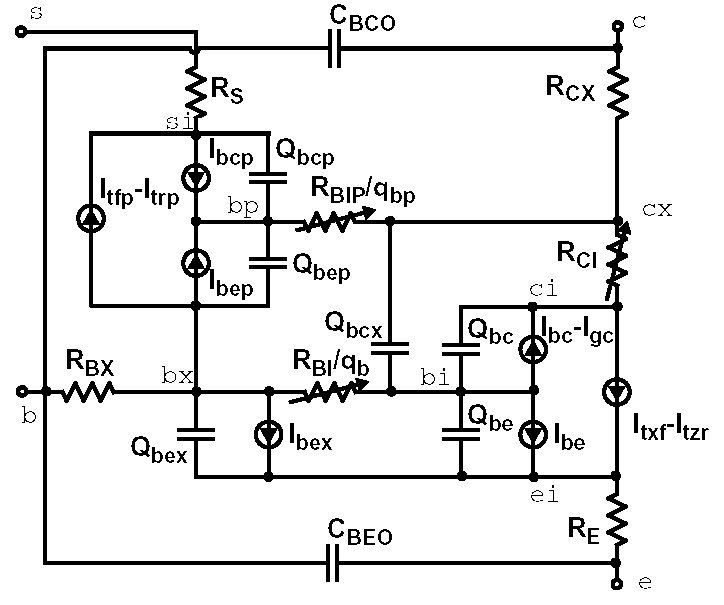
Model Structure
VBIC Parameters
Because the VBIC model is based on SGP model it is possible to start with SGP parameters, carry out some transformations. Following parameters are from VBIC version 1.2, which is implemented in LTSpice in the 4-terminal version without excess phase network and self-heating effect. To switch from SGP to VBIC you should set the extra parameter level to 9.
| Name | Description | Unit | Default |
| Tnom | Parameter measurement temperature | °C | 27. |
| Rcx | Extrinsic collector resistance | Ω | 0.1 |
| Rci | Intrinsic collector resistance | Ω | 0.1 |
| Vo | Epi drift saturation voltage | V | Infin. |
| gamm | Epi doping parameter | 0.0 | |
| hrcf | High current RC factor | Infin. | |
| Rbx | Extrinsic base resistance | Ω | 0.1 |
| Rbi | Intrinsic base resistance | Ω | 0.1 |
| Re | Intrinsic emitter resistance | Ω | 0.1 |
| Rs | Intrinsic substrate resistance | Ω | 0.1 |
| Rbp | Parasitic base resistance | Ω | 0.1 |
| Is | Transport saturation current | A | 1e-16 |
| nf | Forward emission coefficient | 1. | |
| nr | Reverse emission coefficient | 1. | |
| Fc | Fwd bias depletion capacitance limit | 0.9 | |
| Cbeo | Extrinsic B-E overlap capacitance | F | 0.0 |
| Cje | Zero bias B-E depletion capacitance | F | 0.0 |
| pe | B-E built in potential | V | 0.75 |
| me | B-E junction grading coefficient | 0.33 | |
| Aje | B-E capacitance smoothing factor | -0.5 | |
| Cbco | Extrinsic B-C overlap capacitance | F | 0. |
| Cjc | Zero bias B-C depletion capacitance | F | 0. |
| Qco | Epi charge parameter | C | 0. |
| Cjep | B-C extrinsic zero bias capacitance | F | 0. |
| pc | B-C built in potential | V | 0.75 |
| mc | B-C junction grading coefficient | 0.33 | |
| Ajc | B-C capacitance smoothing factor | -0.5 | |
| Cjcp | Zero bias S-C capacitance | F | 0. |
| ps | S-C junction built in potential | V | 0.75 |
| ms | S-C junction grading coefficient | 0.33 | |
| Ajs | S-C capacitance smoothing factor | -0.5 | |
| Ibei | Ideal B-E saturation current | A | 1e-18 |
| wbe | Portion of IBEI from Vbei 1-WBE from Vbex | 1. | |
| nei | Ideal B-E emission coefficient | 1. | |
| Iben | Non-ideal B-E saturation current | A | 0. |
| nen | Non-ideal B-E emission coefficient | 2. | |
| ibci | Ideal B-C saturation current | A | 1e-16 |
| Nci | Ideal B-C emission coefficient | 1. | |
| ibcn | Non-ideal B-C saturation current | A | 0. |
| ncn | Non-ideal B-C emission coefficient | 1. | |
| avc1 | B-C weak avalanche parameter 1 | 1/V | 0. |
| avc2 | B-C weak avalanche parameter 2 | 1/V | 0. |
| isp | Parasitic transport saturation current | A | 0. |
| wsp | Portion of ICCP | 1. | |
| nfp | Parasitic fwd emission coefficient | 1. | |
| Ibeip | Ideal parasitic B-E saturation current | A | 0. |
| ibenp | Non-ideal parasitic B-E saturation current | A | 0. |
| ibcip | Ideal parasitic B-C saturation current | A | 0. |
| ncip | Ideal parasitic B-C emission coefficient | 1. | |
| Ibcnp | Non-ideal parasitic B-C saturation current | A | 0. |
| ncnp | Non-ideal parasitic B-C emission coefficient | 2. | |
| Vef | Forward Early voltage | Infin. | |
| Ver | Reverse Early voltage | Infin. | |
| Ikf | Forward knee current | A | Infin. |
| ikr | Reverse knee current | A | Infin. |
| Ikp | Parasitic knee current | A | Infin. |
| tf | Ideal forward transit time | s | 0. |
| Qtf | Variation of TF with base-width modulation | 0. | |
| Xtf | Coefficient for bias dependence of TF | 0. | |
| Vtf | Voltage giving VBC dependence of TF | V | Infin. |
| Itf | High current dependence of TF | A | Infin. |
| tr | Ideal reverse transit time | sec | 0. |
| Td | Forward excess-phase delay time | Sec | 0. |
| kfn | B-E Flicker Noise Coefficient | 0. | |
| afn | B-E Flicker Noise Exponent | 1. | |
| bfn | B-E Flicker Noise 1/f dependence | 1.0 | |
| Xre | Temperature exponent of RE | 0. | |
| Xrbi | Temperature exponent of RBI | 0. | |
| Xrci | Temperature exponent of RCI | 0. | |
| Xrs | Temperature exponent of RS | 0. | |
| Xvo | Temperature exponent of VO | 0. | |
| Ea | Activation energy for IS | V | 1.12 |
| Eaie | Activation energy for IBEI | V | 1.12 |
| Eaic | Activation energy for IBCI/IBEIP | V | 1.12 |
| Eais | Activation energy for IBCIP | V | 1.12 |
| Eane | Activation energy for IBEN | V | 1.12 |
| Eanc | Activation energy for IBCN/IBENP | V | 1.12 |
| Eans | Activation energy for IBCNP | V | 1.12 |
| Xis | Temperature exponent of IS | 3. | |
| Xii | Temperature exponent of IBEI,IBCI,IBEIP,IBCIP | 3. | |
| Xin | Temperature exponent of IBEN,IBCN,IBENP,IBCNP | 3. | |
| Tnf | Temperature exponent of NF | 0. | |
| Tavc | Temperature exponent of AVC2 | 0. | |
| rth | Thermal resistance | K/W | 0. |
| Cth | Thermal capacitance | Ws/K | 0. |
| Vrt | Punch-through voltage of internal B-C junction | V | 0. |
| Art | Smoothing parameter for reach-through | 0.1 | |
| Ccso | Fixed C-S capacitance | F | 0. |
| qbm | Select SGP qb formulation | 0. | |
| nkf | High current beta rolloff | 0.5 | |
| Xikf | Temperature exponent of IKF | 0. | |
| Xrcx | Temperature exponent of RCX | 0. | |
| Xrbx | Temperature exponent of RBX | 0. | |
| Xrbp | Temperature exponent of RBP | 0. | |
| Isrr | Separate IS for fwd and rev | 1. | |
| Xisr | Temperature exponent of ISR | 0. | |
| dear | Delta activation energy for ISRR | 0. | |
| Eap | Excitation energy for ISP | 1.12 | |
| Vbbe | B-E breakdown voltage | V | 0. |
| nbbe | B-E breakdown emission coefficient | 1. | |
| Ibbe | B-E breakdown current | 1e-06 | |
| Tvbbe1 | Linear temperature coefficient of VBBE | 0. | |
| Tvbbe2 | Quadratic temperature coefficient of VBBE | 0. | |
| Tnbbe | Temperature coefficient of NBBE | 0. | |
| ebbe | exp(-VBBE/(NBBE*Vtv)) | 0. | |
| dtemp | Local Temperature difference | ° | 0. |
| Vers | Revision Version | 1.2 | |
| Vref | Reference Version | 0. |
References:
C. C. McAndrew et al., "Vertical Bipolar Inter Company 1995: An Improved Vertical, IC Bipolar Transistor Model", Proceedings of the IEEE Bipolar Circuits and Technology Meeting, pp. 170 - 177, 1995
C. C. McAndrew et.al., VBIC95, "The Vertical Bipolar Inter-Company Model", IEEE Journal of Solid State Circuits, vol. 31, No. 10, October 1996
C. C. McAndrew, VBIC Model Definition, Release 1.2, 18. Sep. 1999